
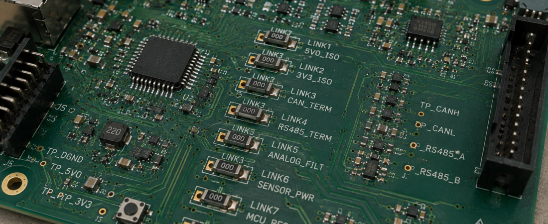
One of the cheapest components on a PCB can also be one of the most useful.
I am talking about the humble 0 Ω resistor.
On a schematic, it can look almost ridiculous. Two nets need to be connected, so instead of simply joining them with copper, I deliberately put a resistor between them whose nominal value is zero.
Electrically, at first sight, it appears to achieve nothing.
But I rarely use a 0 Ω resistor because the circuit needs resistance. I use it because I may want that connection to stop being permanent later.
That is a very different way of looking at it.
Over the years, particularly from working with EMC problems and debugging real electronics rather than just looking at the schematic, I have become much more interested in leaving myself controlled options in a design.
A schematic is created from calculations, datasheets, simulations and assumptions. Then the real PCB arrives. The firmware starts switching things. The actual cable is connected. The sensor behaves slightly differently from the datasheet. A power converter injects something unexpected into the analogue section. A signal edge rings. An EMC test exposes a coupling path that was not obvious on paper.
That is when a tiny 0 Ω resistor can become surprisingly valuable.
For me, a link is not really a resistor.
It is a deliberately designed point of flexibility.
Using links to divide a system into smaller problems
One of the most obvious places I use links is on power rails.
Consider a board with one 5 V supply feeding several functional blocks:
                         +---- 0R ---- MCU / Digital
                         |
5 V regulator -----------+---- 0R ---- Analogue
                         |
                         +---- 0R ---- Communications
                         |
                         +---- 0R ---- Sensor supply
If I only cared about normal operation, those four resistors would be unnecessary.
Everything could simply belong to the same +5V net.
But imagine the first assembled PCB is consuming 180 mA when my estimate suggested something nearer 70 or 80 mA.
Without those isolation points, I have one big problem:
The board is consuming too much current.
With the links, I can remove them one at a time and turn it into several much smaller problems.
I might measure:
MCU / Digital          29 mA
Analogue               14 mA
Communications         18 mA
Sensor supply         116 mA
Now I am not searching the entire board.
I know exactly where to concentrate.
I can also remove a link and place an ammeter directly across its pads. If I know during schematic design that a particular current may be interesting, I sometimes make sure the footprint is accessible enough to probe comfortably.
It is a very small design decision, but it can save a surprising amount of time later.
I have had enough occasions debugging hardware where the alternative is cutting a track, lifting a component or inserting a wire into a place that was never intended to be modified.
Those techniques are perfectly normal during development.
But if I can avoid them by spending fractions of a penny on a link, I normally will.
Separating the regulator from everything it powers
I particularly like having a removable connection immediately after a power converter.
For example:
12 V
 |
Buck converter
 |
0R
 |
3V3_SYSTEM
That single resistor creates several useful test configurations.
With it fitted:
On-board regulator -> real PCB loadWith it removed:
On-board regulator -> no downstream loadAnd with an external supply connected downstream:
Bench PSU -> 3V3_SYSTEMThat becomes extremely useful if something on the rail is behaving strangely.
Suppose I am seeing unwanted noise in an analogue measurement and I suspect that the switching converter is involved.
Without an isolation point, the regulator and its load are electrically tied together.
With the link removed, I can power the downstream circuitry from a clean laboratory supply.
If the noise disappears, I have learned something useful immediately.
If it remains, I have learned something useful as well.
I can also test the converter without the system load and see whether the regulator itself is stable.
That is one of the principles I try to follow when designing hardware:
Make it possible to divide a complicated system into simpler electrical blocks.
Links are one of the easiest ways of doing that.
EMC work made me appreciate links even more
This is probably where my opinion of them changed most.
When a product fails an EMC test, the fastest route to the solution is often experimentation.
You may have a strong theory about where the emissions are coming from, but you still need to prove it.
I do not want every experiment to require:
- cutting traces,
- lifting IC pins,
- soldering components in mid-air,
- or waiting for another PCB revision.
Sometimes the change I want to test is very small.
Imagine:
MCU GPIO ---- 0R ---- external driverFunctionally, the line is completely fine.
But on the oscilloscope I see considerable ringing.
The data rate may only be 1 MHz, so it is tempting to think of it as a slow signal.
But the edge rate is what interests me.
If that GPIO has a 2 ns rise time, a useful rule of thumb for the approximate bandwidth associated with the edge is:
BW ≈ 0.35 / tr
where tr is the rise time.
So, for tr = 2 ns:
BW ≈ 0.35 / (2 × 10⁻⁹)
which gives:
BW ≈ 175 MHz
So even though the GPIO may only be switching at 1 MHz, its fast 2 ns edges contain significant frequency content extending well into the hundreds of megahertz.
This is why a signal that looks “slow” from a firmware point of view can still create very real signal-integrity and EMC problems on the PCB.
That high-frequency energy is what interacts with PCB traces, cable harnesses, connector structures and parasitic capacitances.
If I already have a series resistor footprint close to the source, I can replace the 0 Ω part with:
22 Ω
33 Ω
47 Ω
and measure the result.
A relatively small source resistance can reduce the initial current step, damp reflections and reduce ringing.
In some cases it can also reduce radiated emissions significantly.
Not because the resistor is acting as a traditional low-pass filter in the simple RC sense, but because it changes the source impedance and modifies the edge behaviour.
I do not necessarily know during the first schematic revision whether the optimum value will be 0 Ω, 22 Ω or 47 Ω.
The footprint lets me make that decision based on the real waveform.
That is exactly the sort of flexibility I like designing in.
The data frequency is not necessarily the frequency that matters
This is worth emphasising because it is something I have seen misunderstood many times.
A digital bus running at 500 kHz is not automatically a 500 kHz EMC problem.
If the transitions are sharp, the harmonic content extends much higher.
A useful rule of thumb is:
fknee ≈ 0.35 / tr
where tr is the rise time.
For a 5 ns transition:
fknee ≈ 0.35 / (5 × 10⁻⁹) ≈ 70 MHz
For a 1 ns transition:
fknee ≈ 0.35 / (1 × 10⁻⁹) ≈ 350 MHz
This is why slowing an edge that does not need to be fast can be beneficial.
If a communication interface only requires a few megahertz of bandwidth, there is often no advantage in launching a 1 ns edge into the PCB.
Sometimes a few tens of ohms in series are all that is needed.
But again, I prefer to measure rather than assume.
And that is where the link footprint earns its place.
A link position can become something else entirely
Another thing I like doing is creating a component position that is not necessarily committed to being a 0 Ω resistor forever.
For example:
3V3_DIG ---- [OPTION] ---- 3V3_ANALOGThe initial build may contain:
0 Ωbut the same footprint could potentially become:
Ferrite bead
Small resistance
DNP
depending on what testing tells me.
Suppose the analogue circuitry is initially powered directly from the digital 3.3 V rail.
During testing I discover that high-frequency digital activity is coupling into a sensitive measurement.
Now I already have a controlled location where I can evaluate a ferrite bead.
I am careful here, because ferrite beads are often treated as if they are magic noise absorbers.
They are not.
Their impedance is strongly frequency dependent.
They have DC resistance.
Their impedance can change with DC bias.
Together with capacitors on either side, they can create resonant networks.
So I would not automatically replace the 0 Ω resistor with a ferrite simply because I saw noise.
I would first understand what frequency range is causing the problem and whether the bead’s impedance is useful in that range.
But because the footprint exists, I can perform the experiment cleanly.
That is much better than discovering during EMC testing that the only way to insert a bead is to cut a power trace.
Links are extremely useful for disabling whole sections
Another question I often ask during design is:
Would I ever want to run the board without this section?
Imagine:
3V3 ---- 0R ---- sensor analogue front endor:
MCU_ENABLE ---- 0R ---- peripheral enableIf that subsystem later behaves unexpectedly, I can isolate it.
This is useful for investigating:
- excessive current consumption,
- startup problems,
- bus contention,
- power sequencing,
- noise coupling,
- unexpected interrupts,
- faulty peripherals,
- firmware problems.
There is something very powerful about being able to say:
Let us completely remove this block from the problem and see whether everything else behaves correctly.
That is much cleaner than trying to infer the same thing while everything remains electrically interconnected.
Again, the link is really creating an intentional circuit boundary.
Links as a product-variant tool
They can also become useful once the board moves beyond the prototype stage.
Suppose one PCB has to support two product variants.
One uses RS-485.
Another uses CAN.
Instead of maintaining two completely separate bare PCBs, it may be possible to design:
                       +---- RS-485 transceiver
MCU communication -----|
                       +---- CAN transceiver
and define the hardware through population.
Variant A:
RS-485 path      FITTED
CAN path         DNP
Variant B:
RS-485 path      DNP
CAN path         FITTED
Links can route enables, isolate unused drivers or configure terminations.
The same strategy can work for:
- optional sensors,
- different analogue ranges,
- alternative communications,
- optional memory,
- different power outputs,
- customer-specific functions.
This can reduce the number of bare PCB types that need to be ordered and stocked.
But I think there is an important warning here.
Flexibility has a cost
I do not believe in putting 0 Ω resistors everywhere.
A flexible PCB can very quickly become a configuration nightmare.
If there are thirty links determining what the product actually is, somebody has to control those thirty positions.
That means:
- more BOM variants,
- more assembly instructions,
- more inspection requirements,
- more opportunities for manufacturing errors,
- more documentation,
- more complexity for whoever has to understand the design five years later.
So I try to distinguish between useful flexibility and speculative flexibility.
For every link I add, I want to be able to explain why it exists.
Can it isolate a meaningful block?
Can I measure something useful through it?
Is the component value realistically likely to change?
Does it support a genuine product variant?
Would it simplify EMC testing?
If not, then I probably do not need it.
Ground links require much more thought
Ground is one area where I am particularly careful.
You sometimes see:
AGND ---- 0R ---- DGNDor:
Circuit GND ---- 0R ---- ChassisThere can be completely valid reasons for making ground or chassis connections configurable.
I have certainly found it useful during EMC investigations to have control over where chassis, shield or circuit ground connections are made.
But I never treat a 0 Ω resistor as a magic grounding solution.
At high frequency, current does not simply follow the route that looks shortest on the schematic.
It follows the path of lowest impedance.
For a fast signal travelling above a continuous reference plane, the return current tends to concentrate beneath the signal trace because that minimises loop inductance.
If I create a split in the plane underneath the signal, the return current has to take a detour.
That increases loop area.
And increased loop area usually means:
- more radiated magnetic field,
- greater susceptibility,
- poorer signal integrity.
So:
Signal ----------------------------->
===================================== Ground plane
is not electrically equivalent at high frequency to:
Signal ----------------------------->
=========== gap =====================
               |
               0R
even though the schematic may show both ground regions connected.
This is something my EMC background has made me particularly conscious of: the schematic tells me what is connected; the PCB tells me how the current actually flows.
Those are not always the same thing.
Termination links are another obvious use
Communication interfaces are a natural place for configurable components.
Take RS-485.
Depending on where a node sits on the network, I may or may not require termination.
So instead of permanently fitting a 120 Ω resistor, I may provide a configurable position.
Likewise for fail-safe biasing.
That gives me options for:
- termination fitted,
- termination omitted,
- bias fitted,
- bias omitted.
The hardware can then be assembled according to the system architecture.
I like this approach because the PCB remains common while the final assembly becomes configurable.
But again, configuration control matters.
A flexible design is only good if production knows exactly which options belong to which product.
Sometimes a 0 Ω link becomes a current shunt
A useful development trick is replacing a link temporarily with a low-value resistor.
Suppose I have:
Supply ---- 0R ---- subsystemFor normal units, I populate 0 Ω.
During characterisation, I might fit: 0.1 Ω instead.
If the subsystem draws 250 mA, and I replace the 0 Ω link with a 0.1 Ω resistor, the voltage across it can be calculated using Ohm’s law:
V = I × R
So:
V = 0.25 A × 0.1 Ω = 0.025 V = 25 mV
That 25 mV drop is easy to measure with a multimeter or oscilloscope, giving me a simple way to characterise the current consumption of that part of the circuit.
The power dissipated in the resistor is:
P = I² × R
Therefore:
P = 0.25² × 0.1 = 0.00625 W = 6.25 mW
which is negligible in this particular case.
It is a simple way of characterising current without modifying the PCB.
Obviously for larger currents I need to choose the shunt and package properly, but the principle is useful.
0 Ω does not actually mean zero
It is also worth remembering that a zero-ohm resistor is still a real physical component.
It has:
- finite resistance,
- package inductance,
- parasitic capacitance,
- a maximum current,
- a maximum power dissipation.
For most low-current digital signals, these characteristics barely matter.
For high-current rails or RF, they can.
Suppose a 0 Ω component has an effective resistance of 20 mΩ and carries 3 A.
The voltage drop across the link is calculated using Ohm’s law:
V = I × R
For a current of 3 A and an effective link resistance of 20 mΩ (0.02 Ω):
V = 3 A × 0.02 Ω = 0.06 V = 60 mV
The power dissipated in the link is:
P = I² × R
So:
P = 3² × 0.02 = 0.18 W = 180 mW
That may be significant for a small SMD package.
And 60 mV can be a substantial part of the tolerance on a low-voltage rail.
Likewise, I would not casually insert an ordinary 0603 link into a carefully controlled RF transmission line and assume it behaves like perfect copper.
Its pads, package and discontinuity are part of the transmission structure.
At sufficiently high frequency, even a “short circuit” needs to be treated as a real component.
One of the best reasons for links: the first PCB is not always perfect
This is probably the most human part of the subject.
The first revision of a PCB is not always perfect.
Mine certainly are not always perfect.
Sometimes the real hardware shows me that:
- a pull-up should be removed,
- a peripheral needs isolating,
- a signal needs damping,
- an analogue rail needs different filtering,
- a termination strategy needs changing,
- a block is injecting noise,
- a feature should become optional.
If I already left a sensible link, the modification may take a few minutes.
If I did not, I may be cutting traces, lifting pins or soldering wires onto tiny pads.
I have done those things plenty of times during development, and they are often what teaches me where the next design should be more flexible.
A lot of good design habits do not come from a textbook.
They come from remembering the last board that was painful to debug.
The principle I follow
I do not think the lesson is:
Put 0 Ω resistors everywhere.
That would simply create unnecessary complexity.
My approach is:
If there is a realistic chance that I may need to measure, isolate, configure or tune a connection later, I try to give myself a clean way of doing it.
Sometimes that means:
- a 0 Ω resistor,
- a solder bridge,
- a DNP footprint,
- a test point,
- an optional ferrite position.
The implementation is secondary.
The important part is thinking about the future experiment while I am still designing the PCB.
When I place a link, I ask myself:
What useful thing can I do with this later that I could not do if this were simply copper?
If the answer is:
- isolate a rail,
- measure current,
- disable a subsystem,
- tune a signal,
- test a ferrite,
- change termination,
- support another product variant,
- investigate an EMC issue,
- recover cleanly from an unexpected problem,
then the link has earned its place.
A schematic is not only a description of how a circuit is supposed to work.
For me, a good schematic should also make the circuit easier to understand when reality does something slightly different from what I expected.
That is the real power of links.