
There are some electronics problems that are obvious when you see them.
A shorted rail is obvious.
A missing clock is obvious.
An ADC acquisition-time problem is not.
This is one of those parameters that I think is very easy to overlook, particularly when working with microcontroller ADCs. You can check the analogue voltage with a multimeter and it looks perfect. The resistor-divider calculation is correct. The reference is correct. The ADC code looks fine.
And yet the converted value is slightly wrong.
Or even more confusingly, the first conversion is wrong and the second one looks better.
When I am working with analogue measurements in embedded systems, that sort of behaviour immediately makes me suspicious of the complete analogue path into the ADC, not just the ADC itself.
One of the things I want to know is:
Did the ADC actually have enough time to acquire the voltage I am trying to measure?
That sounds like a simple question.
There is quite a lot hiding behind it.
The ADC pin is not quite what it looks like on the schematic
When I first look at a circuit such as:
Sensor ───── ADC
it is very easy to think of the ADC input almost like a multimeter.
There is a voltage on the pin. The ADC measures it.
Simple.
But that is not really what happens inside many SAR ADCs, including the ADC peripherals commonly integrated into microcontrollers.
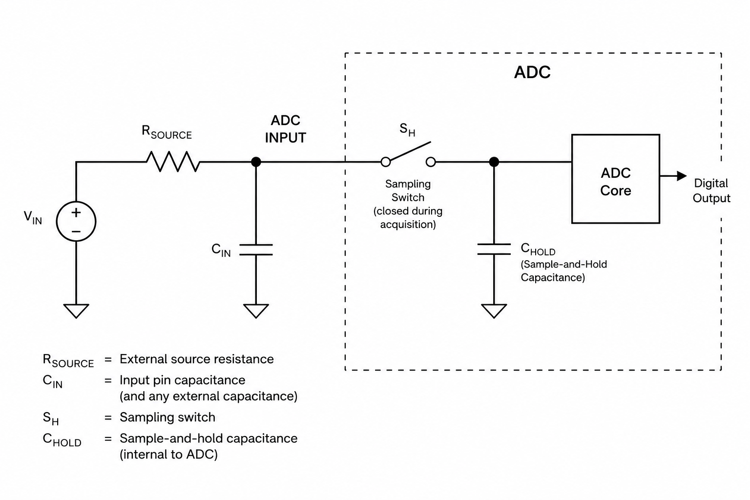
A simplified input looks more like this:
                         Inside ADC

VIN ── Rsource ── switch ──+── ADC core
                            |
                          Chold
                            |
                           GND
There is an internal sample-and-hold capacitor.
During the acquisition period, the internal switch closes and this capacitor has to charge to the voltage present at the ADC input.
Then the switch opens.
The converter performs its conversion using the voltage stored on that capacitor.
That changes the way I think about the input completely.
The ADC is not simply asking:
“What voltage is on my pin?”
It is effectively asking:
“What voltage did my internal capacitor manage to reach before I disconnected it?”
And those two answers are not necessarily identical.
This is why checking the ADC pin with a multimeter can be misleading
This is one of the things I find particularly interesting about this problem.
Imagine I measure the ADC pin and get:
2.000 V
Perfect.
I can leave the multimeter there and it remains at 2.000 V.
It is very tempting to conclude that if the ADC reports something different, the problem must be in the ADC or in the firmware.
But the multimeter and the ADC are not measuring the node in the same way.
The multimeter is looking at a relatively static voltage.
The ADC is periodically connecting an internal capacitor to that node and asking the external circuit to charge it within a limited amount of time.
That is a dynamic event.
If the source impedance is high enough, the ADC can disturb the node during the acquisition period.
The DC voltage can be absolutely correct while the sampled voltage is not.
That distinction is important.
Source impedance is where things start getting interesting
Suppose I have a sensor feeding the ADC through a relatively large resistance:
Sensor ── 100 kΩ ── ADC
When the ADC sampling switch closes, its internal capacitor needs to charge through that resistance.
The charging follows the familiar RC behaviour.
A useful simplified expression is:
Vcap(t) = Vfinal × (1 – e^(-t / RC))
The remaining error is:
Verror = Vstep × e^(-t / RC)
where:
R is the effective source resistance seen by the ADC
C is the ADC’s effective sampling capacitance
t is the acquisition time
Nothing particularly exotic is happening.
It is just capacitor charging.
The important part is that the conversion starts before we have infinite time available.
If the capacitor has not settled sufficiently when the sampling switch opens, the ADC converts the wrong voltage.
And the ADC can be doing its job perfectly.
The first sample after changing channel is particularly interesting
This is where multiplexed microcontroller ADCs can produce some very confusing results.
Suppose I am measuring two channels:
CH0 = 3.0 V
CH1 = 0.2 V
The ADC samples CH0 first.
Its internal sampling capacitor charges to approximately 3.0 V.
The ADC multiplexer then switches to CH1.
That same capacitor now has to move from approximately 3.0 V down to 0.2 V.
That is a 2.8 V step.
If CH1 is driven from a low-impedance source, no problem.
The capacitor charges or discharges very quickly.
But if CH1 comes through a high-value resistor network, the acquisition period may end before the capacitor has reached 0.2 V.
Perhaps the first result corresponds to:
0.27 V
Then I sample CH1 again.
Now the capacitor is starting at 0.27 V rather than 3.0 V.
The next result might correspond to:
0.202 V
That is the sort of behaviour that can send you looking through firmware for a bug that may not actually be there.
And this explains the famous “discard the first ADC reading” trick
I have seen this approach many times in embedded code:
Select ADC channel
Read ADC
Discard result

Read ADC again
Use result
And often it works.
There is a reason.
The first acquisition has already moved the internal sample capacitor much closer to the new channel voltage.
So the second acquisition has a much smaller voltage step to deal with.
I do not think there is anything fundamentally wrong with discarding the first sample when the architecture requires it.
But I prefer to understand why it is necessary.
If I simply add an extra conversion until the numbers look right, I may be hiding a front end that is operating with very little settling margin.
Sometimes the better solution is:
increase the acquisition time
reduce the source impedance
add a local capacitor
buffer the signal
It depends on the application.
Resolution makes the problem less forgiving
The higher the ADC resolution, the closer the sampling capacitor has to get to its final voltage.
For an N-bit ADC:
1 LSB = VFS / 2^N
If I want the acquisition error to remain below approximately half an LSB after a full-scale change, then the settling requirement becomes roughly:
t > RC × (N + 1) × 0.693
That gives a useful feel for the numbers.
For a 12-bit ADC:
t ≈ 9 × RC
For a 16-bit ADC:
t ≈ 11.8 × RC
That is something I always find worth remembering.
A higher-resolution ADC does not only give me smaller digital steps.
It also means the analogue front end has to settle much more accurately.
There is little point buying extra ADC resolution if the analogue node never reaches the required voltage before every conversion.
A practical example
Take a 12-bit ADC with an internal sampling capacitance of approximately:
10 pF
and suppose the effective source resistance is:
50 kΩ
The RC time constant is:
RC = 50,000 × 10 pF
which gives:
RC = 0.5 µs
For around half-LSB settling on a 12-bit ADC, I want roughly nine time constants:
Tacq ≈ 9 × 0.5 µs
So:
Tacq ≈ 4.5 µs
If I configure the ADC so that the acquisition window is only 1 µs, I cannot reasonably expect that node to settle to full 12-bit accuracy after a large voltage transition.
What I like about this example is that nothing is “broken”.
The ADC is fine.
The resistor is fine.
The capacitor is fine.
The firmware is running.
The design simply asks the analogue network to do something faster than the physics allows.
And Rsource is rarely just one resistor
This is another place where I try not to simplify the circuit too much.
Suppose I am measuring a 0–10 V signal through a divider:
VIN
 |
22 kΩ
 |
 +──── ADC
 |
10 kΩ
 |
GND
At first glance, somebody might say that the ADC source resistance is 22 kΩ.
It is not.
Looking back into the divider, the Thevenin resistance is:
Rsource = 22 kΩ || 10 kΩ
which is approximately:
6.9 kΩ
But even that may not be the complete answer.
I may also have:
sensor output resistance
an input-protection resistor
analogue-multiplexer resistance
internal ADC switch resistance
filtering components
When I am trying to understand acquisition behaviour, I care about the complete impedance seen by the sampling capacitor.
Not just the most obvious resistor on the schematic.
This is where protection and measurement design start interacting
A typical sensor input might have a resistor added for protection.
For example:
Sensor ── 10 kΩ ── protection ── ADC
That 10 kΩ may be there for a very good reason.
Maybe I want to limit current during an overvoltage condition.
Fine.
But electrically, I have also just increased the ADC source impedance.
If the sensor and divider already present 20 kΩ, I may now effectively have something approaching:
30 kΩ
driving the sampling network.
That may still be perfectly acceptable.
But I want it to be deliberate.
This is why I do not really like thinking of:
protection
filtering
ADC acquisition
scaling
as separate little schematic blocks.
They all interact through the same analogue node.
RC filters can make acquisition worse — and better
Most analogue inputs I design contain some filtering.
Something like:
              R
Signal ─────/\/\─────+──── ADC
                     |
                     C
                     |
                    GND
At first sight, R makes the acquisition problem worse.
It increases source impedance.
Correct.
But the capacitor changes the picture.
If C is placed close to the ADC input, it can behave as a local charge reservoir.
When the sampling switch closes, the tiny internal ADC capacitor can take much of its charge from this external capacitor rather than pulling it instantly through the entire upstream resistance.
This is why I often think of the capacitor beside an ADC input as doing more than simple noise filtering.
It can also be part of the ADC driver network.
Suppose:
Chold = 10 pF
and I have:
Cfilter = 1 nF
at the ADC input.
The external capacitor is about 100 times larger than the internal sampling capacitor.
The charge taken by Chold therefore produces a relatively small disturbance at the ADC input node.
That can help enormously.
But then bandwidth enters the discussion
Of course, I cannot simply put a huge capacitor on every ADC pin.
For a simple RC low-pass filter:
fc = 1 / (2 × π × R × C)
If I increase C significantly, I reduce bandwidth.
That may be exactly what I want for a slow pressure or temperature measurement.
It may be completely unacceptable for a faster signal.
A larger capacitor can also increase startup time and create another issue if an op-amp is driving the node.
This is why I prefer designing the filter and ADC interface together, rather than treating them as two unrelated jobs.
Driving a SAR ADC with an op-amp is not always trivial either
If the source impedance is too high, an obvious solution is:
Sensor ── filter ── op-amp buffer ── ADC
Now the ADC sees a low output impedance.
That usually makes acquisition much easier.
But I have traded one problem for another.
A SAR ADC input is a switched-capacitor load.
Every acquisition causes a brief current pulse as the internal capacitor is connected.
Some op-amps are perfectly happy with that.
Some are not.
I have learned through analogue and EMC work to be suspicious of circuits that are described simply as “high impedance input” or “capacitive load” without looking at what happens dynamically.
An ADC can present a surprisingly aggressive load for a short instant.
That is why a practical ADC driver often looks like:
                Riso
Op-amp ───────/\/\──────+──── ADC
                         |
                         C
                         |
                        GND
The resistor isolates the op-amp from the switched-capacitive input.
The capacitor provides local charge to the ADC.
The amplifier then replenishes that capacitor between samples.
It is a very simple network, but the resistor and capacitor values need to be chosen with:
the ADC
the op-amp
the required bandwidth
the sample rate
all in mind.
Firmware is genuinely part of the analogue circuit here
This is one aspect of embedded electronics that I really like.
Sometimes the solution costs absolutely nothing in hardware.
Many microcontrollers allow the ADC sample or acquisition time to be selected in firmware.
Conceptually, I might have options such as:
2 ADC clocks
4 ADC clocks
8 ADC clocks
16 ADC clocks
32 ADC clocks
If I am reading a battery voltage once every second, why would I insist on the minimum possible acquisition time?
There is no prize for converting the battery voltage at 1 MSPS.
If increasing the sampling period gives the analogue node plenty of time to settle, I will happily do that.
This is where hardware and firmware stop being separate disciplines.
The analogue source impedance and the firmware ADC configuration are part of the same design.
I think that is easy to forget.
Channel order is another useful debugging tool
If I suspect acquisition problems, one simple experiment is changing the order in which channels are sampled.
Imagine:
CH0 = 2.8 V
CH1 = 2.9 V
CH2 = 3.0 V
Those are small steps.
Now compare it with:
CH0 = 3.0 V
CH1 = 0.1 V
CH2 = 2.9 V
The second sequence asks the sampling capacitor to make much larger voltage transitions.
If CH1 suddenly develops a larger error after I change the sequence, that tells me something very useful.
Nothing in the analogue hardware has changed.
Only the starting voltage on the ADC sampling capacitor has changed.
That is a strong clue that I should investigate acquisition and settling.
I like these sorts of tests because they help isolate the mechanism rather than simply hiding the symptom.
Source impedance also creates leakage errors
Even if I make the acquisition time very long, I still do not like extremely high-impedance ADC inputs without checking leakage.
Suppose:
ADC input leakage = 100 nA
and:
Rsource = 100 kΩ
Then:
Verror = Ileak × Rsource
So:
Verror = 100 nA × 100 kΩ
which gives:
Verror = 10 mV
Now take a 12-bit ADC operating from 3.3 V.
One LSB is:
3.3 V / 4096 ≈ 0.806 mV
So a 10 mV error represents more than 12 ADC counts.
At that point, I cannot really blame the ADC.
The analogue design has made the leakage current significant.
And eventually even the PCB becomes part of the resistor network
This is something that becomes increasingly important with high-impedance analogue inputs.
At a few hundred ohms, a tiny leakage path across the PCB means nothing.
At hundreds of kilohms or megohms, contamination starts becoming more interesting.
Things such as:
flux residue
moisture
board contamination
protection-device leakage
nearby high-voltage nodes
can start contributing measurable currents.
Again, it depends on the required accuracy.
For a rough battery monitor it may be irrelevant.
For a precision sensor channel it may not be.
That is why I always try to think in terms of the measurement system, rather than the nominal ADC resolution alone.
What I actually look at in the datasheet
The headline specification might say:
12-bit ADC, 1 MSPS
Useful.
But when I am designing the analogue input, that is not the information I am most interested in.
I want to find:
sample-and-hold capacitance
input switch resistance
recommended maximum source impedance
minimum acquisition time
ADC clock limits
input leakage
multiplexer behaviour
requirements after switching channels
Sometimes the manufacturer even provides the internal equivalent circuit.
I like those diagrams because they explain immediately why the recommended source impedance exists.
A specification such as:
Maximum recommended source impedance: 2.5 kΩ
is not there because somebody liked the number 2.5 kΩ.
It is connected to the sampling architecture and the time available to charge the internal capacitor.
How I would investigate a suspicious ADC channel
When an analogue channel gives me a result I do not quite trust, I prefer simple experiments before making major changes.
I would try things such as:
Increase the acquisition time.
Does the reading move closer to the expected value?
Read the same channel several times.
Does the first result differ from the following results?
Change the ADC channel order.
Does the error depend on the voltage of the previous channel?
Temporarily lower the source impedance.
Does the error disappear?
Look at the RC network at the ADC pin.
Is there enough local capacitance?
Check the actual ADC timing configuration.
Not what I thought I configured — what the peripheral is actually doing.
Those experiments usually tell me far more than simply staring at the ADC result and wondering whether the converter is “a bit inaccurate”.
I like leaving a little flexibility around ADC inputs
This follows the same philosophy I use elsewhere in PCB design.
I often like having something like:
                 R
Signal ────────/\/\─────+──── ADC
                         |
                         C
                         |
                        GND
Even if the first PCB uses:
R = 0 Ω
C = DNP
I have left myself somewhere to tune the interface.
After measuring the real sensor and the real PCB, I might decide on:
R = 100 Ω
C = 1 nF
or:
R = 1 kΩ
C = 10 nF
or leave it exactly as it was.
The important thing is that I can make the experiment without redesigning the board.
I have become increasingly fond of this approach over the years: calculate what I can before the PCB is built, but leave sensible options for the things that can only really be understood once the hardware exists.
The part I think is easiest to forget
If I had to reduce the whole subject to one idea, it would be this:
An ADC conversion does not start with the ADC core. It starts with charging a capacitor.
Everything upstream influences whether that happens correctly:
sensor impedance
resistor dividers
protection resistance
filters
op-amps
ADC multiplexer resistance
sampling capacitance
acquisition timing
A circuit can therefore be completely correct from a DC point of view and still be wrong dynamically.
That is what makes acquisition-time problems so easy to miss.
The multimeter says the voltage is correct.
The schematic says the voltage is correct.
The maths says the divider is correct.
But for a few microseconds inside the ADC, the voltage may not yet be where we think it is.
And sometimes the difference between an ADC that gives slightly mysterious readings and one that behaves exactly as expected is simply this:
Give that tiny internal capacitor a little more time to charge.