
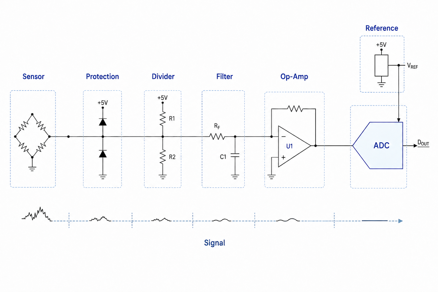
There is something about ADC specifications that can give a false sense of security.
12-bit ADC.
16-bit ADC.
24-bit ADC.
The number sounds impressive, and it is very easy to mentally translate more bits into more accuracy.
I try not to do that.
From my own work with sensors, analogue electronics and embedded systems, I have learned to be much more suspicious of everything that happens before the ADC.
Because by the time the signal finally reaches the converter, quite a lot may already have happened to it.
A typical measurement path might look like:
Sensor
  |
Protection
  |
Scaling
  |
Filter
  |
Op-amp
  |
ADC
And there is another signal entering the ADC that is just as important:
Voltage reference
      |
      v
     ADC
Every one of those blocks can introduce error.
The ADC cannot know that.
It simply converts the voltage presented to it.
If I give a 16-bit ADC a voltage that is already 0.5% wrong, I do not get a 16-bit accurate measurement.
I get a very high-resolution digital representation of a voltage that is 0.5% wrong.
That distinction is fundamental.
Resolution and accuracy are two very different things
Take an ideal 16-bit ADC operating over a 0–5 V range.
The number of possible codes is:
2^16 = 65,536
So one LSB is approximately:
5 V / 65,536 = 76.3 µV
That sounds fantastic.
A change of only 76 µV can theoretically move the result by one count.
But suppose the analogue scaling network before the ADC has a gain error of 0.2%.
At a 5 V full-scale equivalent input, 0.2% represents:
5 V × 0.002 = 10 mV
And 10 mV corresponds to roughly:
10 mV / 76.3 µV ≈ 131 ADC counts
Suddenly those 16 bits do not look quite as magical.
The ADC resolution is still 16 bits.
But the system accuracy is being limited somewhere else.
This is why, when I look at a measurement circuit, I prefer to ask:
Where can the signal change between the sensor and the digital result?
That question is much more useful than simply asking how many bits the ADC has.
Start at the sensor
The first source of uncertainty may already exist before the signal reaches my PCB.
Suppose I have a pressure sensor specified as:
Accuracy: ±0.5% full scale
No amount of ADC resolution downstream can recover information that the sensor itself does not provide accurately.
If I then design an analogue front end with another ±0.5% error, my measurement system clearly cannot be described meaningfully as “16-bit accurate”.
This seems obvious when written down.
But I think it is surprisingly easy during component selection to become focused on the electronics and forget that the measurement chain starts at the physical quantity itself.
For me, the real chain is:
Physical quantity
      |
   Sensor
      |
Electrical signal
      |
Analogue front end
      |
     ADC
      |
   Firmware
      |
Displayed value
Every stage matters.
Protection components are not invisible
The next thing the signal often meets is protection.
This might include:
series resistors
TVS diodes
clamp diodes
RC networks
input protection ICs
These components are there for good reasons.
Anything connected to a cable can be exposed to ESD, overvoltage, transients and incorrect wiring.
But protection components still have electrical characteristics.
A protection diode may have leakage current.
A TVS diode may have significant capacitance.
A series resistor introduces impedance.
For a low-impedance industrial voltage signal, this may barely matter.
For a high-impedance precision measurement, it can matter a lot.
For example, imagine an input protection device leaks:
1 µA
and my source impedance is:
100 kΩ
The resulting error can be:
Verror = I × R
So:
Verror = 1 µA × 100 kΩ = 100 mV
That would be catastrophic for many measurements.
Even 100 nA through 100 kΩ gives:
10 mV
This is one reason I never like looking at protection as a separate box that simply sits “in front of” the measurement circuit.
It is part of the measurement circuit.
Then comes scaling
A lot of sensor interfaces need some form of voltage scaling.
Suppose I want to measure a 0–10 V signal with a 3.3 V ADC.
A simple divider could be:
VIN
 |
22 kΩ
 |
 +------ ADC
 |
10 kΩ
 |
GND
The nominal ratio is:
10 / (22 + 10) = 0.3125
So:
10 V → 3.125 V
Everything looks straightforward.
But now look at the resistor tolerances.
If I use 1% resistors, R1 and R2 are not guaranteed to be exactly 22 kΩ and 10 kΩ.
Worst case, one can move high while the other moves low.
For example:
R1 = 22.22 kΩ
R2 = 9.90 kΩ
The divider ratio becomes:
9.90 / (22.22 + 9.90) ≈ 0.3082
Instead of 0.3125.
That is roughly a 1.4% ratio error from the nominal divider.
The ADC can be perfect and my result is already wrong.
This is why the tolerance of a divider cannot really be assessed by saying:
“They are 1% resistors.”
What matters is the ratio.
Ratio tracking matters
Temperature makes this more interesting.
Suppose the board moves from 20°C to 70°C.
That is a 50°C change.
If a resistor has a temperature coefficient of:
50 ppm/°C
its possible change over that range is:
50 ppm × 50 = 2500 ppm
which is:
0.25%
If both divider resistors move by exactly the same percentage, the ratio barely changes.
But if they track differently, the gain of the measurement changes.
This is one reason I like matched resistor networks in precision applications.
Sometimes I care less about whether the resistance is exactly 10.000 kΩ and more about whether two resistors move together.
That is a subtle but important distinction.
The filter can also change the measurement
Then I normally have some filtering.
A simple example:
             R
Signal -----/\/\-----+---- ADC
                     |
                     C
                     |
                    GND
At DC, the capacitor looks irrelevant.
But in a real measurement system, bandwidth and noise are part of accuracy.
If the filter bandwidth is too wide, I may digitise noise that was never part of the useful sensor signal.
If it is too narrow, I may distort the signal I actually want.
The resistor tolerance and capacitor tolerance also determine the real cutoff frequency.
The ideal equation is:
fc = 1 / (2 × π × R × C)
If R is ±1% but the capacitor is an X7R part with a nominal ±10% tolerance, the actual filter corner is not exactly where the schematic says it is.
And ceramic capacitors introduce another issue that I think is often underestimated:
capacitance changes with DC bias.
A capacitor marked 100 nF may not behave like 100 nF at its actual operating voltage.
For decoupling this may be completely acceptable.
For a precision filter whose response matters, I want to know.
Then the signal reaches the op-amp
This is where a lot of small errors can begin to accumulate.
An op-amp can contribute:
input offset voltage
input bias current
offset drift
gain error
finite open-loop gain
common-mode error
noise
PSRR limitations
output swing limitations
Take input offset voltage.
Suppose my amplifier has:
Vos = 500 µV
That sounds tiny.
For a 5 V full-scale signal:
500 µV / 5 V = 0.01%
Still small.
But if I am measuring a sensor signal of only 100 mV before applying gain, that same 500 µV represents:
500 µV / 100 mV = 0.5%
Now it is no longer tiny.
The importance of an error depends entirely on where in the signal chain it appears.
Gain multiplies some errors too
Suppose I use a non-inverting amplifier with a gain of 10.
An input-referred offset of 500 µV can appear as approximately:
5 mV
at the output.
Now the ADC sees that 5 mV as if it were real signal.
Again, the ADC has no way of knowing otherwise.
This is why I prefer thinking in terms of input-referred error when I am building an error budget.
I want every error expressed in terms of the physical input if possible.
That makes it much easier to compare one contribution against another.
Bias current can become important with large resistor values
Input bias current is another parameter that can look insignificant until it meets a high-impedance circuit.
Suppose:
Ibias = 100 nA
and the effective resistance at the input is:
100 kΩ
Then:
Verror = 100 nA × 100 kΩ = 10 mV
That can easily dominate a precision measurement.
This is why I do not select an op-amp from its offset specification alone.
A device with fantastic offset but relatively large bias current may be a poor choice for a high-impedance sensor.
The circuit and component have to be considered together.
Noise deserves a slightly different way of thinking
Noise is interesting because unlike a simple offset or gain error, it changes continuously.
An op-amp might specify input voltage noise in:
nV/√Hz
That means the total RMS noise depends on the bandwidth over which I allow that noise into the system.
Very roughly:
Vrms ≈ Noise density × √Bandwidth
for a flat noise density over the band.
So if I unnecessarily allow 100 kHz of bandwidth into a sensor whose useful information only extends to 20 Hz, I am allowing far more noise into the measurement than I need.
That is why filtering is not just a nice extra.
It is part of the noise design.
One lesson from EMC work that has stayed with me is that I always want to ask:
What bandwidth does this signal actually need?
Anything outside that bandwidth is potentially something I do not need to measure.
The reference voltage is effectively another analogue input
I think voltage references deserve much more attention than they sometimes receive.
For a typical ADC:
ADC code ∝ VIN / VREF
So if VREF moves, the conversion result moves.
Imagine a 16-bit ADC using a 2.5 V reference specified at:
±0.1% initial accuracy
That alone represents:
2.5 V × 0.001 = 2.5 mV
One LSB of the 16-bit converter is:
2.5 V / 65,536 ≈ 38.1 µV
So the initial reference tolerance corresponds to around:
2.5 mV / 38.1 µV ≈ 66 LSB
Again, the ADC can have enormous resolution while another component determines the absolute accuracy.
Of course, calibration can remove much of the initial reference error.
But temperature coefficient and long-term drift remain important.
Reference noise becomes ADC noise
The reference is also not simply a perfect DC voltage.
Real references have:
broadband noise
low-frequency noise
output impedance
thermal drift
load regulation
transient response
Some SAR ADCs draw short bursts of current from the reference during conversion.
That means the reference must sometimes be treated as a dynamic source, not just a static voltage.
This is why the capacitor around a reference pin can be extremely important.
And again, PCB layout enters the problem.
A beautiful 2.5 V reference IC can still produce a poor ADC result if I route noisy digital return currents through the same piece of copper used by the reference return.
The schematic’s GND symbol is not zero volts everywhere
This is probably one of the most important practical lessons I have taken from EMC and mixed-signal design.
On the schematic:
GND
means one net.
On the real PCB, every piece of copper has:
resistance
inductance
So if current flows through it, there is a voltage difference.
At DC:
V = I × R
At higher frequency, the inductive component can become even more important.
Suppose a digital circuit produces a transient current of 100 mA through a ground path with only 20 mΩ resistance.
Even ignoring inductance:
V = 0.1 A × 0.02 Ω = 2 mV
For a 16-bit 2.5 V ADC:
1 LSB ≈ 38 µV
That 2 mV ground movement corresponds to more than:
50 LSB
The physical current path matters.
This is why I am always careful with analogue ground, reference return paths and where high-current digital or switching currents flow.
The schematic can say everything is connected to GND.
The electrons still need an actual path through the copper.
Then, finally, we arrive at the ADC
Only after all of that do I start worrying about the converter itself.
The ADC contributes its own errors:
offset error
gain error
INL
DNL
quantisation
thermal noise
reference coupling
acquisition errors
All of those matter.
But I find that there is sometimes too much focus on the ADC specification while relatively little attention is paid to the chain driving it.
A 16-bit converter with ±2 LSB INL may sound like a major concern.
But if my resistor divider is already wrong by 0.2%, that divider corresponds to around:
131 LSB
on a 16-bit scale.
Clearly I should fix the divider before worrying about whether the ADC is ±1 or ±2 LSB.
Acquisition time belongs in this discussion too
I wrote separately about ADC acquisition time because I think it deserves its own discussion.
But it is also part of this error chain.
The voltage reaching the ADC pin may be correct while the voltage reaching the ADC’s internal sampling capacitor is not.
If the source impedance is too high and acquisition time too short, I get another error before conversion.
That is another example of why I do not like thinking of the ADC as a passive voltmeter.
The analogue front end and ADC input architecture interact.
This is why I like building an error budget
For any measurement where the accuracy genuinely matters, I like to write the main errors down.
It does not need to become an enormous mathematical exercise.
Even a simple table is incredibly useful.
Imagine something like:
Sensor accuracy               ±0.50%
Divider ratio                 ±0.10%
Amplifier gain/offset         ±0.05%
Voltage reference             ±0.05%
ADC error                     ±0.03%
Temperature effects           ±0.10%
The first thing this tells me is where my problem actually is.
If my sensor itself is ±0.5%, spending a large amount of money reducing ADC error from ±0.03% to ±0.01% probably achieves very little.
On the other hand, if I have an accurate calibrated sensor and my divider uses ordinary 1% resistors, then the resistor network may deserve much more attention.
The error budget helps me spend engineering effort in the right place.
I think that is one of its biggest benefits.
Worst case and RSS are not the same thing
If I simply add all maximum errors:
0.50 + 0.10 + 0.05 + 0.05 + 0.03 + 0.10 = 0.83%
That gives a conservative worst-case result.
For independent random errors, it may be reasonable in some circumstances to use root-sum-square:
Total = √(E1² + E2² + E3² + …)
Using the same example gives a significantly smaller number.
But I am careful here.
Not every specification represents a random independent error.
Tolerance limits, systematic offsets and temperature drift cannot always be thrown into an RSS calculation simply because the resulting number looks nicer.
I prefer to understand what each term actually represents.
Calibration can change everything — but not everything
Calibration is extremely powerful.
If I apply two accurately known input values, I can determine a correction of the form:
Corrected value = m × ADC reading + b
where:
b corrects offset
m corrects gain
That can remove a lot of static error from:
resistor ratios
amplifier gain
ADC gain
reference initial tolerance
This is why a circuit built from components that individually have modest absolute tolerances can sometimes produce a very accurate calibrated system.
But calibration is not magic either.
A room-temperature two-point calibration does not automatically correct:
temperature drift
non-linearity
noise
hysteresis
long-term drift
sensor repeatability
So I like calibration very much, but I prefer to think of it as another part of the design rather than a way to excuse a poor analogue front end.
Sometimes repeatability matters more than absolute accuracy
There is another useful distinction.
Suppose a sensor system always reads 1.2% high but is extremely repeatable.
That fixed gain error may be easy to calibrate.
A system that randomly varies by ±0.8% is much harder to improve.
So when selecting components, I do not only ask:
How accurate is it?
I also care about:
repeatability
noise
drift
stability
A repeatable systematic error is often easier to deal with than an unpredictable one.
More bits can actually expose more problems
There is something slightly ironic about moving to a higher-resolution ADC.
It often makes the analogue design look worse.
With an 8-bit ADC over 5 V:
1 LSB ≈ 19.5 mV
A 2 mV ground error is invisible in terms of output codes.
With a 16-bit ADC:
1 LSB ≈ 76 µV
The same 2 mV error is now around:
26 LSB
Nothing got worse electrically.
The ADC simply became good enough to reveal errors that were already present.
I think this is why high-resolution analogue design can sometimes be frustrating.
You do not just buy a better ADC.
You have to make the entire circuit worthy of the ADC.
Component placement also becomes part of accuracy
Once signals become small enough, I stop thinking purely in terms of the schematic.
Where is the reference capacitor physically placed?
Where does its ground return go?
Is the ADC input trace running beside a switching node?
Does the analogue signal cross a split in its reference plane?
Are digital currents sharing copper with the sensor return?
Is a high-impedance input routed underneath a noisy clock?
These questions can matter more than changing a resistor from 0.1% to 0.05%.
This is another area where my EMC experience strongly influences the way I design analogue circuitry.
I am always thinking about current paths, not just voltage nodes.
I have learned not to optimise the wrong component
This is probably the practical lesson I value most.
It is very easy to spend time finding a converter with:
better INL
more bits
lower noise
higher sample rate
because those specifications are easy to compare.
But sometimes the real improvement is something far less exciting:
use a better matched resistor network
reduce the measurement bandwidth
choose an op-amp with lower offset
improve the reference
change the grounding
reduce source impedance
calibrate the system properly
I have learned to look for the dominant error first.
There is very little value improving an error source that contributes 0.01% when another part of the chain contributes 0.5%.
The signal has already travelled a long way before the ADC sees it
This is the way I now tend to visualise an analogue measurement:
Sensor
  |
  |  sensor accuracy / drift
  v
Protection
  |
  |  leakage / impedance
  v
Scaling
  |
  |  ratio tolerance / tempco
  v
Filter
  |
  |  noise / bandwidth / settling
  v
Op-amp
  |
  |  offset / bias / gain / drift
  v
ADC
  ^
  |
Reference
  |
  |  accuracy / noise / drift
The signal accumulates history as it travels.
By the time it arrives at the ADC, the converter is not seeing the perfect physical quantity I started with.
It is seeing the result of every component and every current path before it.
The question I now prefer asking
When somebody tells me:
“It’s a 16-bit measurement.”
I find myself wanting to ask:
16-bit resolution — but what is the actual system accuracy?
Those are very different questions.
The better starting point, in my experience, is:
What measurement accuracy do I actually need at the sensor input, over the operating temperature and over the life of the product?
Then I can work backwards.
How much error can the sensor contribute?
How much can the analogue front end contribute?
How stable does the reference need to be?
How much ADC performance do I really need?
Does calibration make sense?
That approach usually leads to a much more balanced design.
Because ultimately, the ADC can only convert what arrives at its input.
And very often, most of the interesting accuracy problems happened before the signal ever got there.